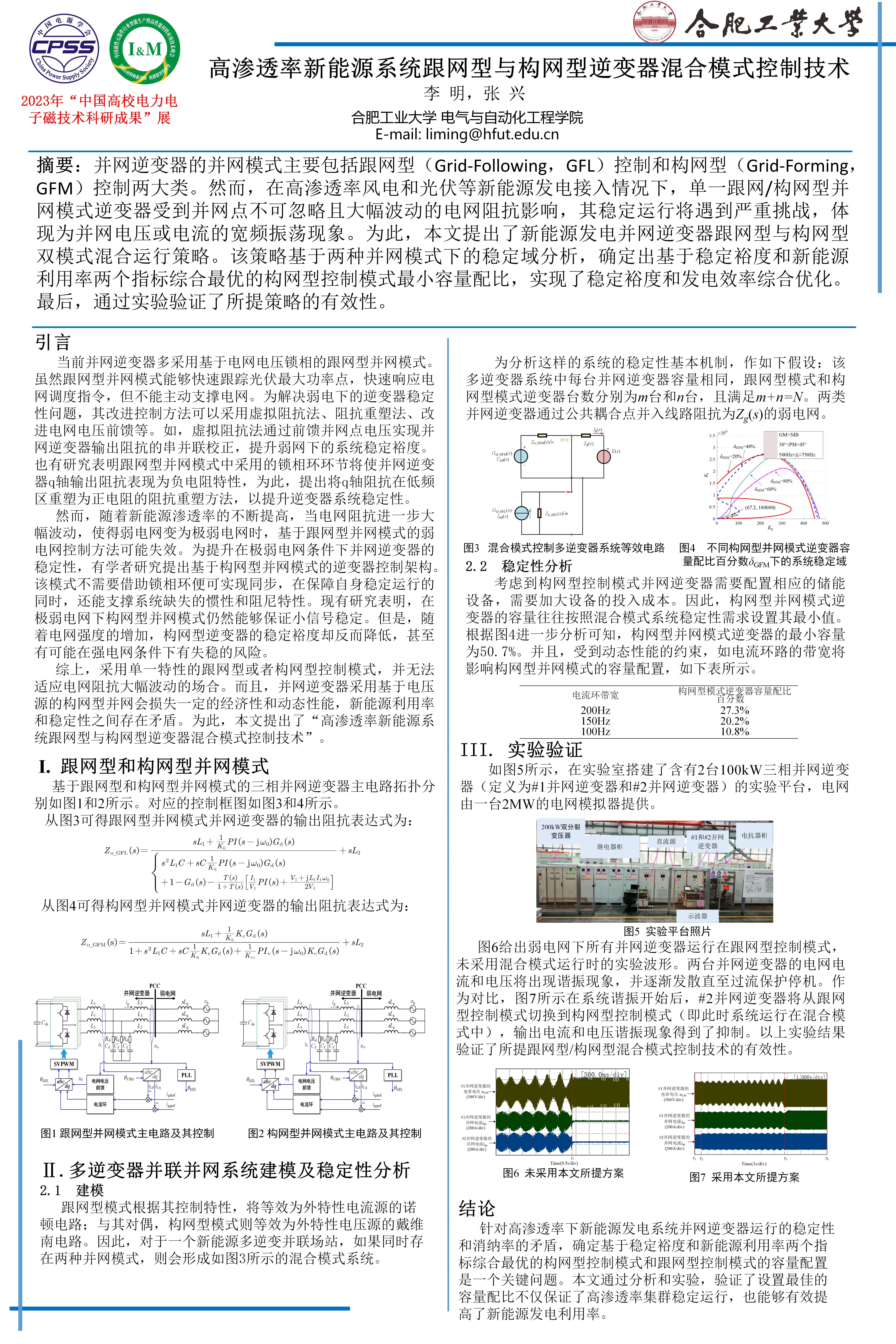
并网逆变器的并网模式主要包括跟网型(Grid-Following,GFL)控制和构网型(Grid-Forming,GFM)控制两大类。然而,在高渗透率风电和光伏等新能源发电接入情况下,单一跟网/构网型并网模式逆变器受到并网点不可忽略且大幅波动的电网阻抗影响,其稳定运行将遇到严重挑战,体现为并网电压或电流的宽频振荡现象。为此,本文提出了新能源发电并网逆变器跟网型与构网型双模式混合运行策略。该策略基于两种并网模式下的稳定域分析,确定出基于稳定裕度和新能源利用率两个指标综合最优的构网型控制模式最小容量配比,实现了稳定裕度和发电效率综合优化。最后,通过实验验证了所提策略的有效性。
2024-09-25
查看详情

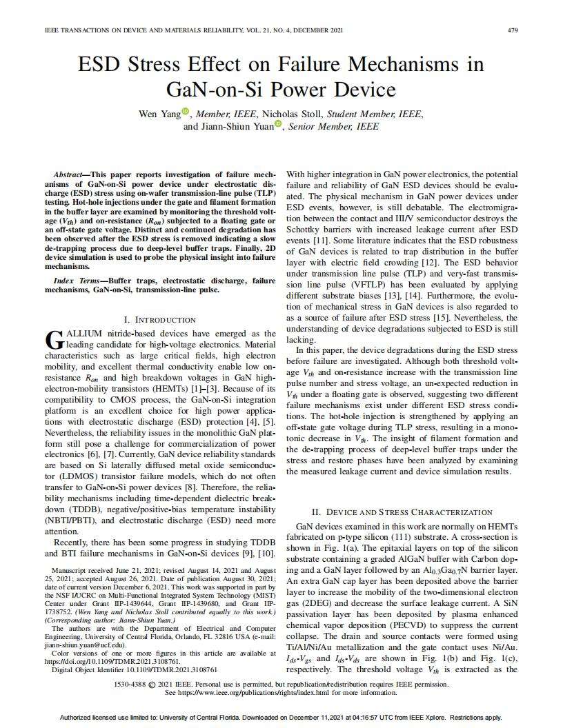
Abstract—This paper reports investigation of failure mechanisms of GaN-on-Si power device under electrostatic discharge (ESD) stress using on-wafer transmission-line pulse (TLP)testing. Hot-hole injections under the gate and filament formationin the buffer layer are examined by monitoring the threshold voltage (Vth) and on-resistance (Ron) subjected to a floating gate oran off-state gate voltage. Distinct and continued degradation hasbeen observed after the ESD stress is removed indicating a slowde-trapping process due to deep-level buffer traps. Finally, 2Ddevice simulation is used to probe the physical insight into failuremechanisms.Index Terms—Buffer traps, electrostatic discharge, failuremechanisms, GaN-on-Si, transmission-line pulse.
2024-09-25
查看详情

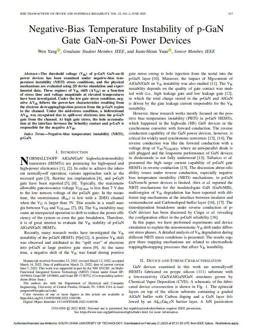
Abstract—The threshold voltage (Vth) of p-GaN GaN-on-Sipower devices has been examined under negative-bias temperature instability (NBTI) stress conditions, and the physicalmechanisms are evaluated using 2D device simulation and experimental data. Three regimes of Vth shift (Vth) as a functionof stress time and voltage magnitude at elevated temperatureshave been investigated. Under the low gate stress condition, negative Vth follows the power-law characteristics resulting fromthe electron de-trapping/injection process from the p-GaN regionto the channel. Under the mid-stress condition, a bidirectionalVth was recognized due to spill-over electrons into the p-GaNgate from the channel. At high gate stress, the hole accumulation at the interface between the Schottky contact and p-GaN isresponsible for the negative Vth.Index Terms—Negative-bias temperature instability (NBTI),p-GaN.
2024-09-25
查看详情

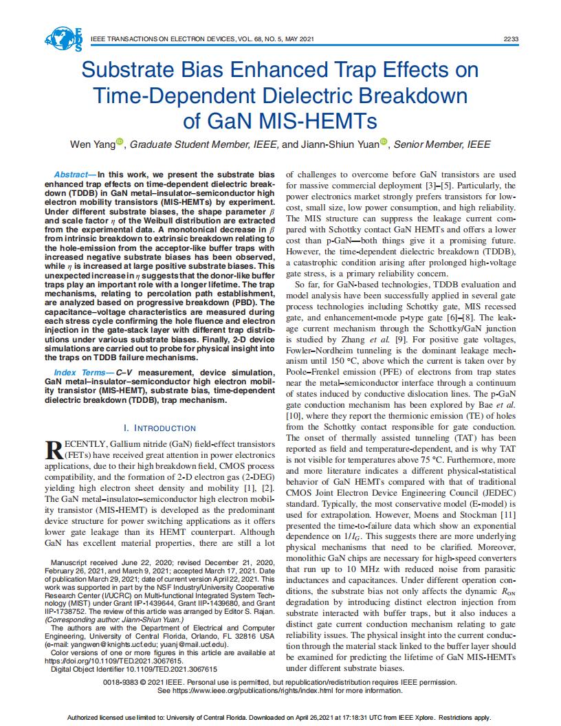
Abstract—In this work, we present the substrate biasenhanced trap effects on time-dependent dielectric breakdown (TDDB) in GaN metal–insulator–semiconductor highelectron mobility transistors (MIS-HEMTs) by experiment.Under different substrate biases, the shape parameter βand scale factor η of the Weibull distribution are extractedfrom the experimental data. A monotonical decrease in βfrom intrinsic breakdown to extrinsic breakdown relating tothe hole-emission from the acceptor-like buffer traps withincreased negative substrate biases has been observed,while η is increased at large positive substrate biases. Thisunexpected increase in η suggests that the donor-like buffertraps play an important role with a longer lifetime. The trapmechanisms, relating to percolation path establishment,are analyzed based on progressive breakdown (PBD). Thecapacitance–voltage characteristics are measured duringeach stress cycle confirming the hole fluence and electroninjection in the gate-stack layer with different trap distributions under various substrate biases. Finally, 2-D devicesimulations are carried out to probe for physical insight intothe traps on TDDB failure mechanisms.Index Terms—C–V measurement, device simulation,GaN metal–insulator–semiconductor high electron mobility transistor (MIS-HEMT), substrate bias, time-dependentdielectric breakdown (TDDB), trap mechanism.
2024-09-25
查看详情

没有更多了